Prev Post
ZHANG RuyunRelated Content


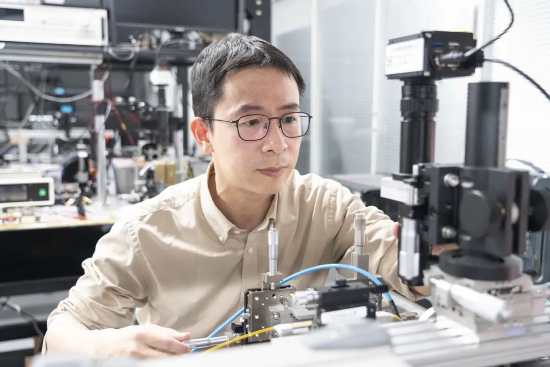
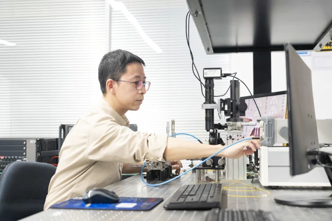
Dr. CHEN Bigeng can often be found in his lab at the Research Center for Frontier Fundamental Studies of Zhejiang Lab (ZJ Lab), where he is busy fixing chips, fine-tuning probes, coupling laser light, and initiating tests.
Dr. CHEN Bigeng received his bachelor's degree in Optoelectronic Information Engineering from Zhejiang University. After graduation, he pursued a doctoral degree at the same university under the guidance of Prof. TONG Limin. Then he worked as a postdoctoral fellow at the University of Southampton, engaged in research on silicon-based integrated optoelectronic devices. Four years later, he returned to China and joined ZJ Lab. For a decade or more, CHEN Bigeng has been working on optics and exploring the limits of optical modulation within a millimeter.
"Light is ubiquitous in nature, which forms illumination, temperature and color in our living space, but it seems illusory and uncontrollable." CHEN Bigeng said, "As science and technology advance, people have gradually learnt more about properties of light. Today, researchers' ability to manipulate light waves has reached such a height, breadth and depth that has never seen before, providing very powerful research methods for related disciplines."
Research on on-chip optoelectronic integrated circuits is significant for both physics and engineering applications, which offers a way to put pure research interests into action. "As Richard Feynman said, 'There is plenty of room at the bottom'. I am convinced that it is promising to study and manipulate light in well‐designed microstructures." Having been thoughtful and ingenious, CHEN Bigeng, as the team leader, often conducts lab tests with team members and provides detailed instructions on performing these tests. Meanwhile, he pays close attention to every little detail in his research.
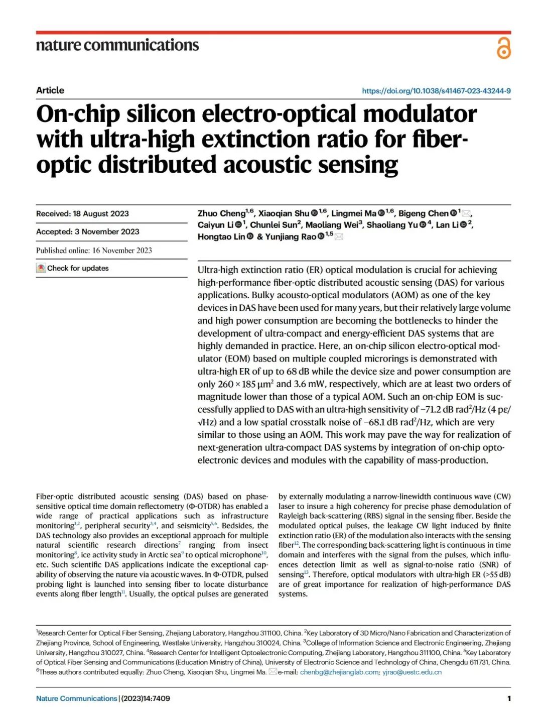
After years of joint efforts, his team developed an on-chip silicon electro-optical modulator (EOM) with an ultra-high extinction ratio for the first time in the world, of which the device size and power consumption are two orders of magnitude lower than those of a conventional high-extinction-ratio modulator. In this way, the optical modulation contrast of the EOM is controlled to a new extreme at sub-millimeter scales. The work is of far-reaching significance to the future development of some highly sensitive optoelectronic systems, and was published in the famous academic journal Nature Communications.
Since ZJ Lab shifted its focus to intelligent computing and explored new frontiers, the team is positioned to research the forefront issues related to the limits of computational power accordingly. "We have entered a new era of sci-tech innovation that is 'computing-intensive, data-driven and model-based'. Computing has changed from an auxiliary tool to an important innovation engine." CHEN Bigeng said, "To implement higher-performance computing systems and build more energy-efficient computational power centers, the interconnects between computing cores, storage, and other nodes must be fast, efficient, reliable and energy-efficient. From our perspective, it is essential to explore the limits of optical modulation in new directions."
To this end, CHEN Bigeng's team focuses on the research and development of optoelectronic integrated modules and systems for high-speed optical interconnects. By developing high-bandwidth-density optical-electrical interfaces and optoelectronic co-packages combined with high-speed electronic chips, copper interconnects are substantially shortened, and the physical challenges in trade-off between transmission rate, distance and power consumption in a traditional inter-chip or inter-board interconnection architecture are solved, so as to further improve computing performance and reduce interconnect power consumption, and provide important technical support for enhancing intelligent computing hardware capabilities and advancing the development of next-generation high-performance computing systems at ZJ Lab.
At present, the team is working to address technical challenges such as the design and testing of large-scale integrated optoelectronic chips, the energy efficiency of optical-electrical interfaces, and co-packaging. "To achieve the goal, we're questing for the limits of bandwidth density, transmission power consumption and integration scale, all within a millimeter," CHEN Bigeng said confidently.


Office of Global Engagement
Follow us
Visit Us